What is a semiconductor package substrate?
Semiconductor packaging materials play an important role in protecting IC chips from the surrounding environment, ensuring electrical connection for chip mount on printed wiring boards.
Demand for high-speed, high-integration and low power consumption of ICs accompanying the rapid progress of electronics technology such as AI, Cloud computing, Intelligentization of automobiles, and due to the miniaturization and thinning of electronic devices typified by smart phone and wearable devices, semiconductor packages are required further high density, multilayer, low-profile. TOPPAN has been developing and manufacturing semiconductor packaging materials by utilizing the cutting-edge photolithography and etching technology, Toppan's group long-established advantages.
Typical semiconductor packages and their structures
-
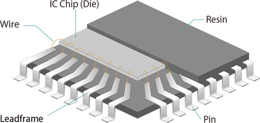
Lead frame
An IC chip (die) cut from a silicon wafer is fixed onto the die pad in the center of the frame. The leads and IC chip are connected with gold wire, etc., and then sealed with mold resin.
-
FC-BGA
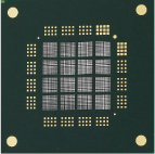
An IC chip (die) cut from a silicon wafer is connected to the solder bumps (protruding connection electrodes) in the center of the substrate and sealed with underfill resin.
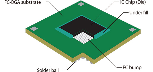
TOPPAN is engaged in the development and manufacture of FC-BGA substrates with ultra-high density interconnect structures that are compatible with the miniaturization of semiconductor processes.
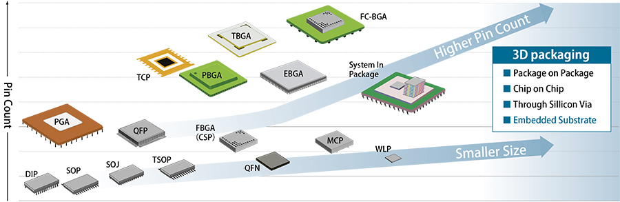
Progress of Semiconductor Packages
Semiconductor packages require 3 points: 1. smaller packaging with high density; 2. high pin-count for high integration with multiple functions; 3. high heat-dissipation characteristics and high electric properties enabling high performance. TOPPAN Inc. offers wide range of products required by constantly evolving needs in the semiconductor packaging market.