Metal etched materials for various applications
Etching is a process involving the selective removal of some portions of metal material by chemically corroding. Using metal etching technology, TOPPAN manufactures and sells various products in addition to semiconductor package related products.
This technology is applied to a variety of areas which include various parts for electronic products, such as antennas for IC cards, inner and exterior parts of devices, and decorative products such as metal bookmarks, calendars, and others.
Characteristics of Etching Products
- Compared to stamping method, etching method applies less stress on the substrate in which demonstrates its suitability for microfabrication.
(No material deformation such as burrs, bend, or warp.) - Etching technology is applied not only for through hole processes, but also for half-etching processes.
- Capable of various types of secondary processing, such as shape profiling (bending / cut-off) surface processing (mirror polishing / coloring / plating) bonding, and insert injection molding.
- Non-conventional design products are welcomed since we have an internal design center.
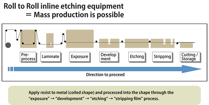
- Produce with Roll to Roll process, therefore, mass production is possible.
- Delivery form could be either roll or sheet.
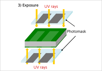
Photo Etching Process
-

Materials are prepared based on the purposes.
-

Remove soluble photoresist.
(Pattern Development) -
Cleaning the material and coating
photoresist on its surface.
(Liquid Photoresist / Dry Film Photoresist) -
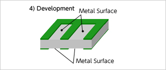
Remove material underneath the soluble
photoresist (have removed) with etching. -

The pattern on the master mask is transferred
via UV ray exposure onto the material. -

Strip the remaining photoresist.
Features of Toppan's group etching line