Large-size conductive glass/ glass substrate
Large size conductive glass substrate is developed by patterning the low resistance copper film on the glass.
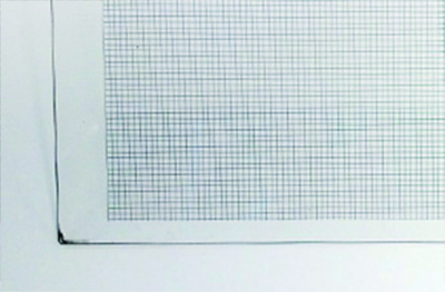
Pattern could be formed on the large size glass substrate of 730mm×920mm at maximum.
Applications such as large size printed circuit boards and large size glass sensors are expected.
Features
- Pattern is formed on the glass substrate using copper with low sheet resistance.
- Processing of large size glass substrate possible
→ 730mm×920mm at maximum
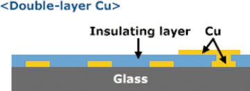
Layer structure

Specifications
Glass size
| Dimension | 730×920mm | 620×750mm | 680×880mm |
|---|
| Thickness | 0.5mm | 0.7mm |
|---|
Patterning on 1st layer
| Cu thickness | 0.30μm |
|---|---|
| Sheet resistance value | 0.1Ω/□ |
| Resolution (L/S) | 10μm/10μm |
Patterning on 2nd layer
| Cu thickness | 0.30μm |
|---|---|
| Sheet resistance value | 0.1Ω/□ |
| Resolution (L/S) | 10μm/10μm |
| Film thickness between layers (Acrylic resin) | 1.0~2.5μm |
| Hole diameter of film between layers | 20μm |
Wiring pattern image (SEM image)
-
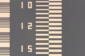
Cu line pattern : 10~15μm
-
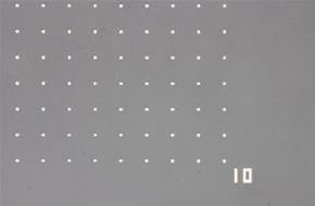
Cu circle pattern : 10μm
- Cu thickness and/or line width can be changed as per customer request.