-
 Apr 2, 2024TOPPAN at embedded world 2024
Showcasing electronics solutions including TOPPAN ORTUSTECH brand TFT displays for industrial devices and LC MAGIC™ light control film
-
 Feb 20, 2024TOPPAN to Participate in Kumamoto Industrial Revitalization Expo 2024
Supporting Kumamoto with DX solutions and manufacturing as the region is revitalized by the semiconductor industry.
-
 Jan 16, 2024TOPPAN at 16th AUTOMOTIVE WORLD
Showcasing light control film for vehicles, the latest small and medium-sized LCDs, and CCMs and MEAs for hydrogen energy
-
 Dec 05, 2023TOPPAN to Build Line for Development and Mass Production of Next-Generation Semiconductor Packages in Ishikawa, Japan
Purchasing land and plant at JOLED Nomi Site as a new base
-
 Sep 08, 2023Toppan’s Liquid Crystal Light Control Film Is World’s First Adopted for Side Windows of Toyota Cars
Collaboration with AGC delivers high-quality light control glass for automobile side windows
-
 Aug 22, 2023Toppan to Participate in Display Innovation China EXPO 2023
Showcasing the latest Blanview™ LCDs delivering high visibility and low power consumption for sectors from mobility to medical devices
-
 Jun 30, 2023TOPPAN Niigata Plant Receives GOLD STATUS in RBA Audit
TOPPAN has acquired GOLD STATUS for the VAP(Validated Assessment Program)Audit with RBA(Responsible Business Alliance)at the Niigata Plant.
-
 Jun 09, 2023TOPPAN to Join IMAGE SENSING SHOW 2023
Showcasing range of ToF applications and demonstrating 20-meter sensing using Hybrid ToF™ sensor
-
 Apr 28, 2023TOPPAN Enters Power Semiconductor Business
Porting and performing wafer manufacturing process for device manufacturers and supporting stable power semiconductor supply with turnkey services from circuit design to manufacture.
-
 Mar 14, 2023TOPPAN Develops Sensing System to Detect Abnormal Sounds at Facilities
New sensors added to solution for automated collection of environmental data and reduction of equipment inspection workload.
-
 March 7, 2023TOPPAN to Showcase Latest Display Solutions at embedded world 2023
In Nuremberg, ORTUSTEC's cutting-edge products will be on display, including the Blanview LCDs and aerial touch displays with a body 50% thinner than previous models.
-
 Jan 19, 2023TOPPAN to Participate in 15th AUTOMOTIVE WORLD
Showcasing new light blocking “black” grade of light control film for vehicles and a range of TOPPAN Group products driving solutions for the automotive industry.
-
 Dec 19, 2022TOPPAN Develops “Black” Light Control Film for Automobiles
New “Normal Black” grade of LC MAGIC™ light control film ensures privacy inside vehicles by blocking 95% of visible light.
-
 Sep 19, 2022EV Group and TOPPAN Photomask join forces to accelerate market adoption of nanoimprint lithography for photonics manufacturing
Joint marketing and technology collaboration will leverage strengths of two market leaders to provide nanoimprint lithography development kits and foster industrial-scale implementation.
-
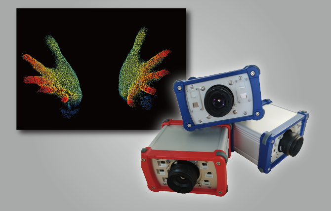
 Jun 16, 2022TOPPAN and Brookman Technology’s Next-Generation Time-of-Flight Sensor Is World’s First Capable of Measuring Distances of up to 30 Meters
World’s first CMOS-process-based Time-of-Flight sensor with maximum outdoor measurement range of 20 meters, more than five times that of existing products, will drive practical use of image sensors and cameras for autonomous drones and other industrial applications.
-
 Apr 01, 2022TOPPAN Carves Out Semiconductor Photomask Business to Launch New Company
TOPPAN Photomask Co., Ltd., the only photomask manufacturer with manufacturing locations in the U.S., Europe, Japan, and Asia coupled with participation from Integral Corporation, will drive further growth and enhance competitiveness as an independent entity and support the semiconductor industry as the world’s merchant photomask market leader.
-
 Jan 18, 2022TOPPAN to Participate in Automotive World
Showcasing the Group’s leading-edge electronics products, from the latest contactless touch panel model to devices that drive digital transformation.
-
 Oct 26, 2021TOPPAN Establishes System for Automated Collection of Environmental Data at Manufacturing Plants
Blind-spot-free communication networks installed at facilities with complex structures to enhance inspection operations and strengthen active environmental conservation efforts.
-
 Oct 07, 2021TOPPAN Develops Technology to Enable Mass Production and Cost Reduction for Microfluidic Chips
LCD manufacturing technology successfully applied to create prototype chips for specimen testing. Mass production can support expanded use of microfluidic chips expected to be used for super-early cancer detection.
-
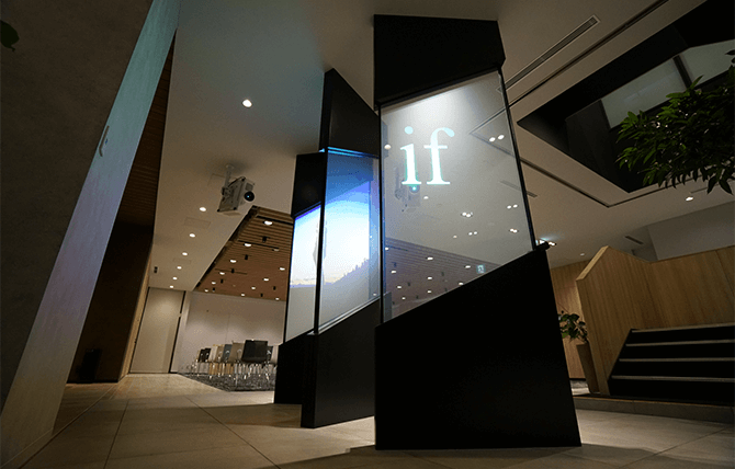
 Sep 15, 2021TOPPAN Significantly Improves Aerial Touch Display and Doubles Viewing Angle
Next-generation model with enhanced image quality adopted for elevator hall at Tokyo Midtown Yaesu, supporting a touchless experience from entrance to office.
-
 May 31, 2021TOPPAN Launches Mass Production of Compact ZETA Communication Modules Enabling Wireless Firmware Updates
Driving integration into key edge devices for digital transformation with modules 25% smaller than conventional models and the release of an add-on board for Sony Semiconductor Solutions’ SPRESENSETM.
-
 Apr 08, 2021TOPPAN Photomasks Receives Supplier Excellence Award from Texas Instruments
 -
 Feb 26, 2021TOPPAN Set to Join embedded world 2021 DIGITAL
Presenting the latest technologies and services, including Blanview TFT-LCDs and aerial touch displays.
-
 Nov 06, 2020 TOPICSTOPPAN to Participate in electronica virtual 2020
Showcasing the new aerial touch display as well as the latest technologies and services
-
 Oct 12, 2020TOPPAN Develops World’s First Aerial Touch Display to Generate Parallel to the Panel
Samples of space-saving display with flat body 50% slimmer than existing products to be made available to medical device and security-related sectors from December
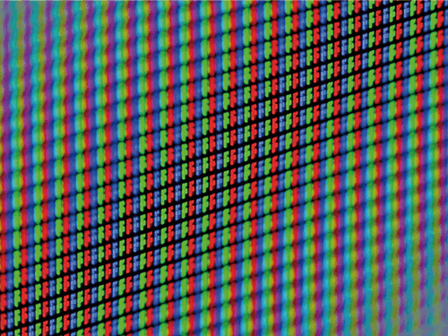
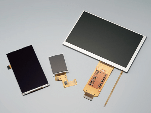
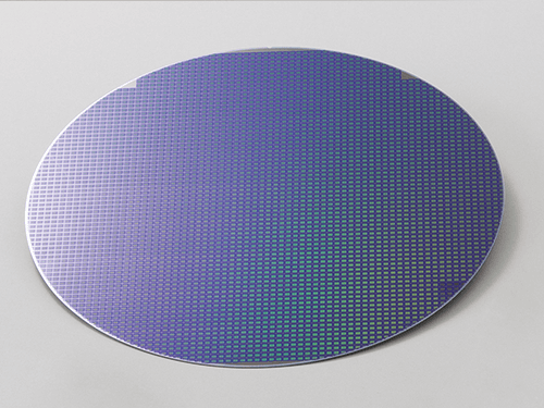
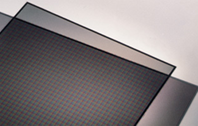
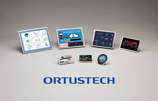
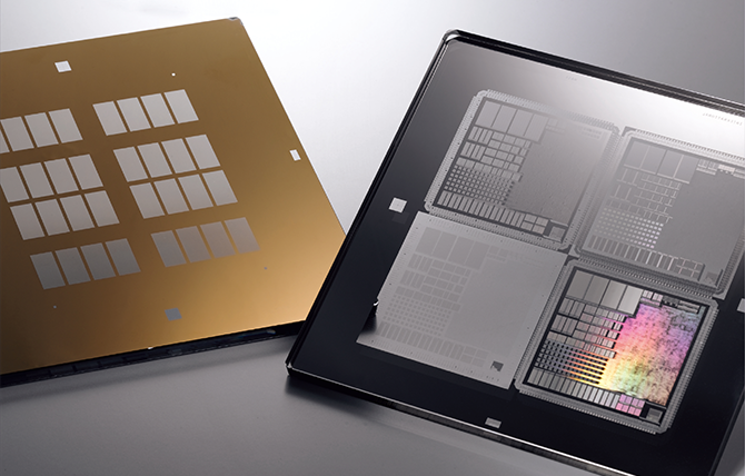
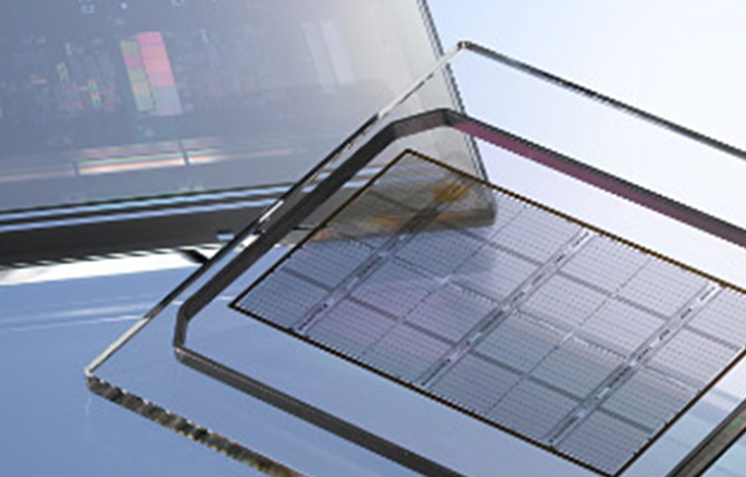
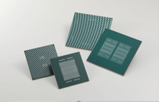
Color filters serve as a pivotal material for image quality of image- output/ input devices, such as displays and image sensors. By using our ultra-fine processing technology based on the plate making technology for printing, patterns of a color filter, microlens or electrodes are formed on glass or silicon wafers.
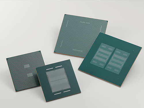
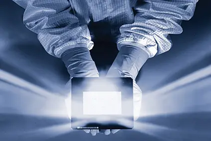
We are working on design and development of various devices by taking advantages of Toppan's group many elemental technologies, such as turnkey service (from design to pilot & mass production of semiconductor circuits), modules for various sensors, light control film and etc..
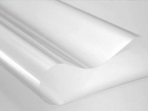
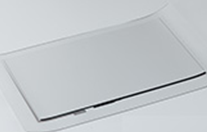
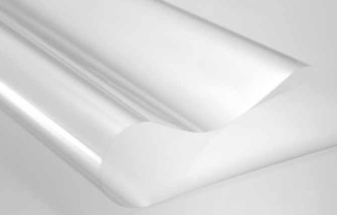
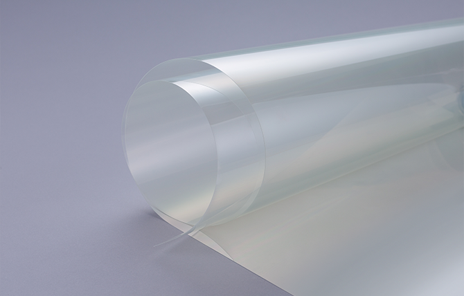
With our precise coating and laminating technologies by micro coater or spatter and material developing technology, we develop and manufacture ultra-fine films patterned with copper touch sensors, anti-reflection films for flat display panels, and LC light-control films allowing a quick changeover between opaque and transparent by a flip of the power switch.
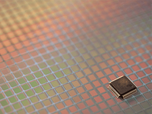
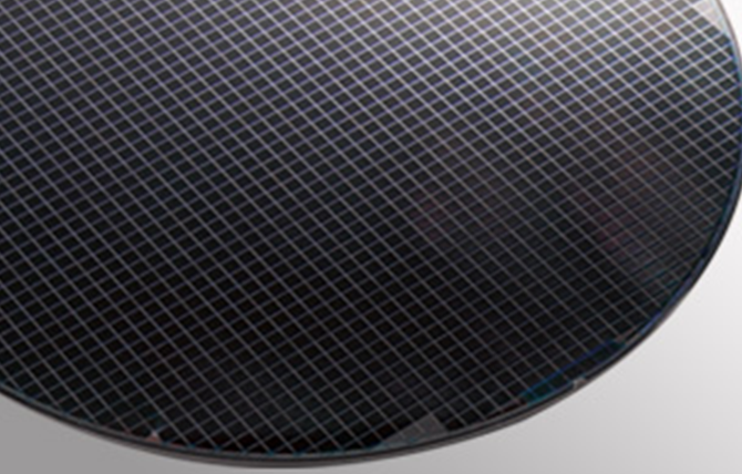
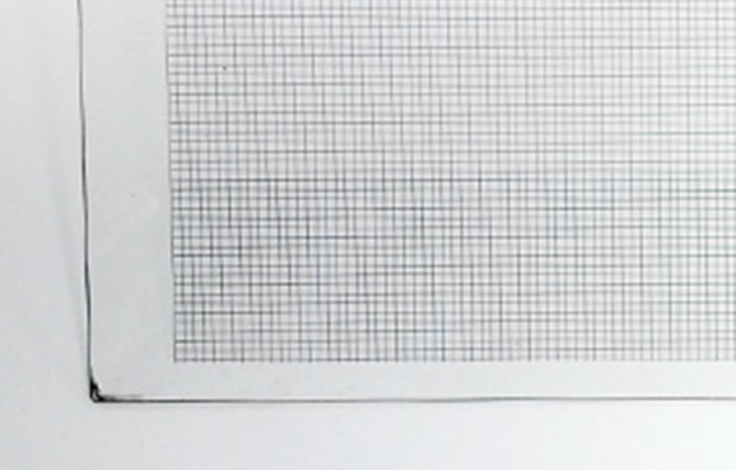
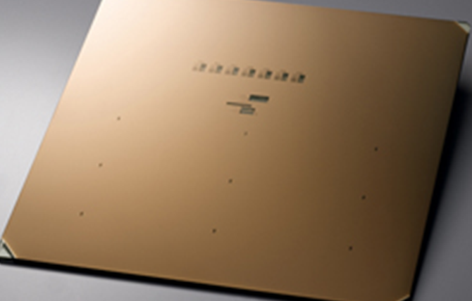
A photomask is a glass plate having a light shielding film on which ultra fine circuit patterns are formed, and used to produce patterns of complicated semiconductor circuits onto silicon wafers. In addition to photomasks for semiconductors, we develop and manufacture glass masks for various studies and development, silicon stencil masks, molds for nanoimprinting, etc.
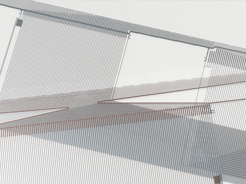
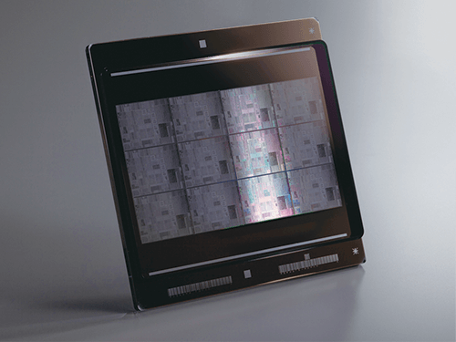
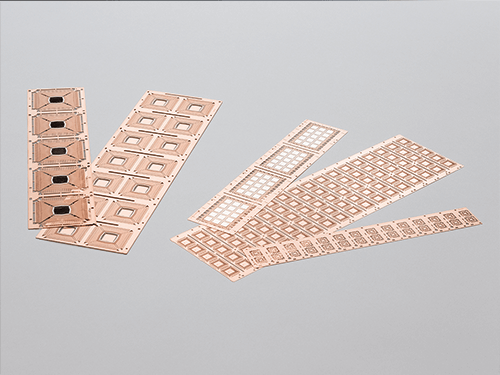
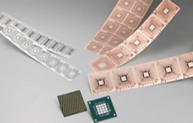
By exploiting our advanced photolithography technology and build-up wiring technology, we are working on development and production of FC-BGA substrates or various lead frames that meet the needs for high-performance and small-sized LSIs.
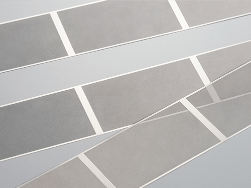
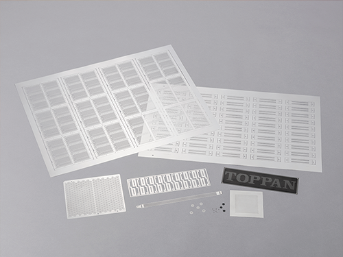
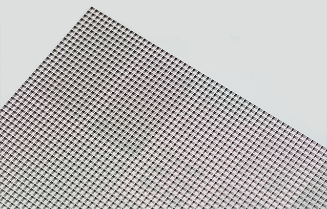
Based on our photo etching technology, we manufacture and sell products for a wide variety of fields, including interior and exterior parts and jigs used for electronics products and various machines.


We are working on design and development of various devices by taking advantages of Toppan's group many elemental technologies, such as turnkey service (from design to pilot & mass production of semiconductor circuits), modules for various sensors, light control film and etc..